ECS-Uniwill OEM F71Ixx (F71ILx), Laptop Motherboard Schematic diagram
|
|
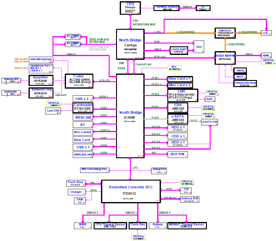
Price: US $17.25 *Power Block Diagram ** Power Sequence Diagram (MoterBoard) ***NB9P/M Power ON/OFF Sequence (VGA) ****USB Board schematic diagram (35GEF5000-C0 / 80GEF5000-C0, F50Ixx) *****Audio Board schematic diagram (35G2F5000-C0 / 80G2F5000-C0, F50Ixx) Major components: CPU : Intel Penryn Clock Generator : ICS952013 + ICS93772 Chipset : Intel Cantiga 965GM/965PM // ICH9-M Video: UMA / nVIDIA (NB9P-GS / NB9M-GS) Audio : ALC662 or ALC888 / APA2068 + APA3010 KBC(Embeded Controller),SIO :ITE8512 LAN Controller :RTL8102E / RTL8111C Card Bus, etc. : JMB380(IEEE1394A), JMB360(e-SATA) , RTS5158E <Power System> APL5331KAC OZ811 OZ8602 OZ8138 APL5331KAC APL5912 OZ815 MAX8770GTL This schematic diagram is applicable to motherboards : F71Ixx 37GF50000-xx 82GF50000-xx 82GF50000-A0 37GF50000-A0 82GF53000-B0F 37GF50000-B0 82GF50000-C0 37GF50000-C0 82GF50000-C0F File type : PDF Language : English |
|---|