Compal OEM LA-D301P B4DBG + (V4DA2 LS-A131P, LS-A133P, B4DBU LS-D301P, LS-D302P, A4DBH LS-B732P, LS-B734P) , motherboard Schematic diagram
|
|
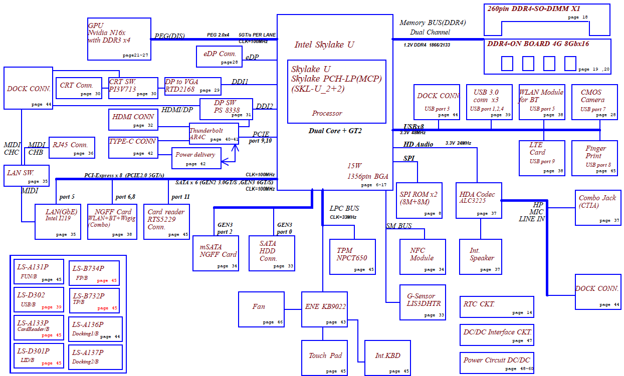
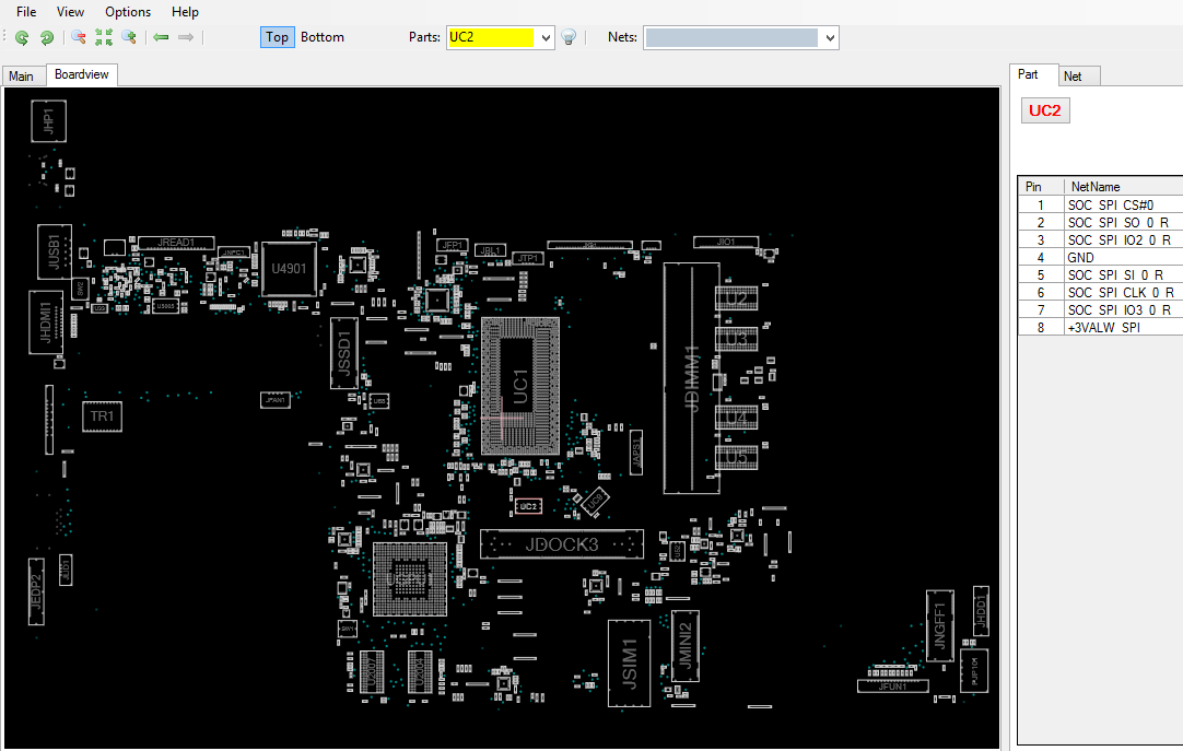
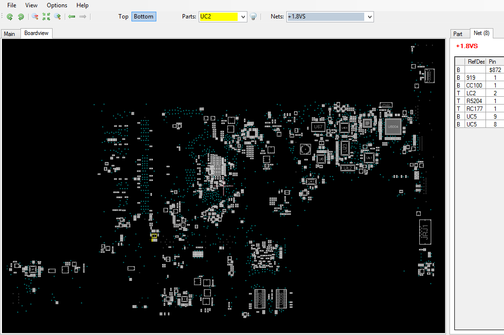
Price: US $18.75 B4DBG LA-D301P Daughter Boards p/n: Function Board (V4DA2 LS-A131P) USB Board (B4DBU LS-D302P) CardReader Board (V4DA2 LS-A133P) LID Switch Board (B4DBU LS-D301P) Finger Print Board (A4DBH LS-B734P) TP Transfer Board (A4DBH LS-B732P) Also included: — Schematic diagram for Function Board (V4DA2 LS-A131P) — Schematic diagram and BoardView file for USB Board (B4DBU LS-D302P) — Schematic diagram and BoardView file for CardReader Board (V4DA2 LS-A133P) — Schematic diagram and BoardView file for LID Switch Board (B4DBU LS-D301P) — Schematic diagram and BoardView file for Finger Print Board (A4DBH LS-B734P) — Schematic diagram and BoardView file for TP Transfer Board (A4DBH LS-B732P) — Power Map — Power Sequence Timing diagram — SMBus Block diagram Major components: CPU: Intel Skylake-U/KabyLake-U + DDR4 GPU: UMA or DIS (Nvidia N16x + DDR3) EC: ENE KB9022 File type : PDF Language : English |
|---|